MEMS technology can integrate any kind of sensors and actuators into TEM.
Thus, I believe our research will make it possible to observe any kind of phenomena with atomic resolution in the future.
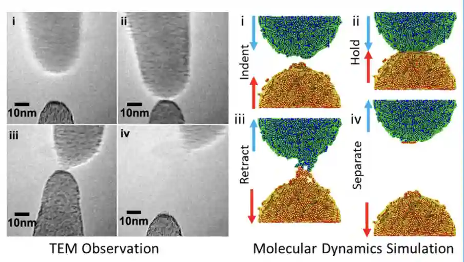
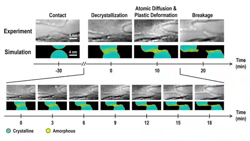
MoS2-MoS2 probes were brought into contact, and then we observed the contact by TEM.
We found that the covalent bonds near the edge of MoS2 plays the significant role to transfer the 2D materials.
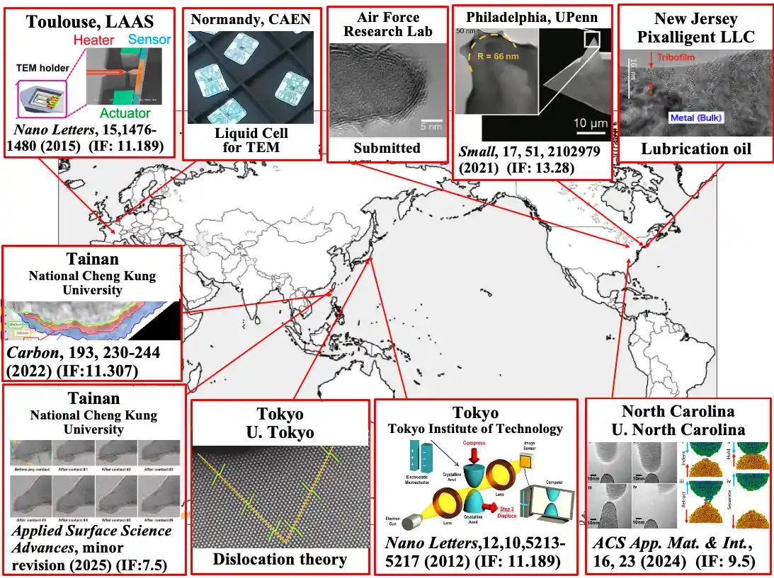
[1] T.R.Sathwik, T. Sato, et.al, ACS Applied Materials & Interfaces, Vol.16, Issue.23, pp.30506-30520 (2024) (Impact factor: 9.5)
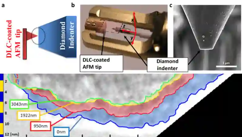
We scratched DLC probes on a flat diamond surface, and related the volume loss to the change in Sp2, Sp3 structure.
We found that when the true stress increases to a certain value, DLC starts to wear.
[2] J-H.Liang, Z.Milne, M.Rouhani, Yi-Pan Lin, R.A. Bernal, T. Sato, et.al. Carbon, 193, pp.230-244 (2022) (IF:11.31)
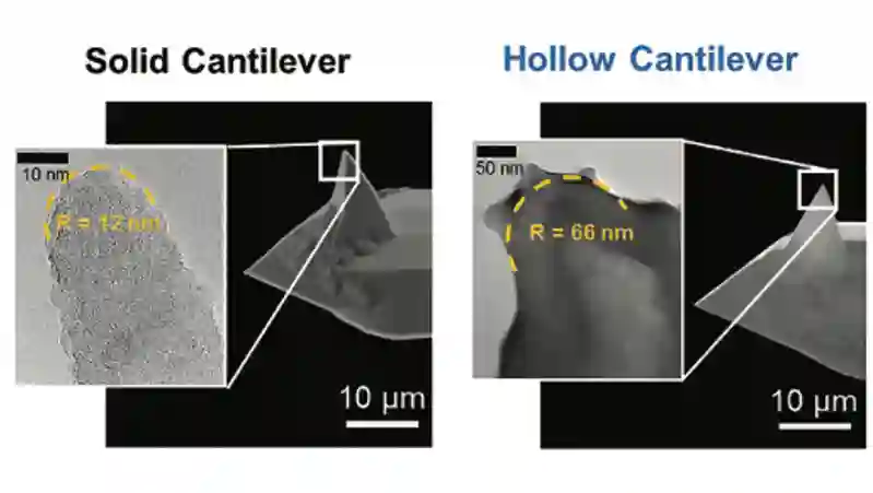
We fabricated the hollow AFM probes using ALD and Xe gas for ultrafast AFM images.
Our TEM technique succeeded in observing the hollow AFM probes.
[3] W.Cha, M.F.Campbell, K.Hasz, S.M.Nicaise, D.E.Lilley, T. Sato, et.al., Small, 17, 51, 2102979 (2021) (IF: 13.28)
We integrated an electrostatic actuator that achieves an ultraslow actuation (=0.1 nm/s).
The technique enabled us to observe a superplasticity in a silicon nanowire.
[4] T.Ishida, T. Sato, et.al., Nano Letters, 15, pp.1476-1480 (2015) (Impact Factor: 11.189)
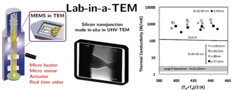
We integrated a heater and a thermal sensor on the MEMS device, and put it into TEM.
That measures the heat transfer in a silicon nanowire. We found a ballistic heat transfer in the silicon nanowire.
[5] L. Jalabert, T. Sato, et.al., Nano Letters, 12, 10, pp.5213-5217 (2012). (IF: 11.189)